Our Comprehensive Services
Explore our diverse range of high-precision measurement solutions. Tailored inspection technologies for all your optical metrology needs.
Strain profiling
Strain in multilayer thin-film compound semiconductors can cause defects, dislocations, and piezoelectric fields, which affect device performance.

Many companies and research institutes are working to reduce this strain. However, since the actual strain distribution in the epi layer cannot be directly measured, improvements are usually confirmed only by observing changes in device performance.
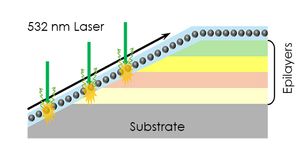
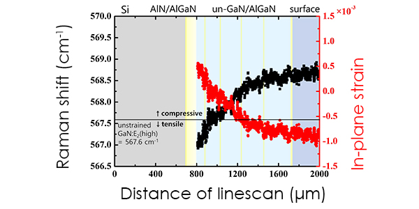
AccuOptotec has developed a method to directly measure strain distribution in multilayer semiconductors using precision diagonal polishing (within 1 degree) and SERS analysis. This technique has been successfully applied to GaN-based blue LEDs, AlGaN DUV-LEDs, and GaN-on-Si power semiconductors, providing meaningful results.
This is the only method that directly verifies strain effects and improvements, making it a breakthrough in semiconductor research.


High speed sub-micron thermal imaging

Try Our Thermal Imaging Technology– High speed sub-micron thermal imaging service
We provide high-resolution thermal imaging services using our advanced semiconductor equipment. Ideal for customers who want to experience the technology before purchasing, our service offers precise thermal measurements across a wide range of applications. Discover the performance of our system firsthand—accurate, reliable, and tailored to your needs.
EL-PL measurement
Applications of EL-PL Measurement
- Performance testing, defect analysis, and material optimization.
- Solar Cells: Evaluating charge carrier dynamics and identifying efficiency losses.
- Semiconductor Research: Investigating new materials and device structures for improved performance.
- Interquantum efficiency, external quantum efficiency measurement
- Temperature dependent (3K-300K), time-resolved measurement
AccuOptotec’s Advanced EL-PL Measurement Technology
AccuOptotec has developed a high-precision EL-PL measurement system that enhances analysis speed and accuracy. Our technology enables simultaneous EL-PL measurement, allowing for a more comprehensive evaluation of semiconductor properties in real-time.With cutting-edge optical analysis methods, AccuOptotec provides high-resolution, non-destructive EL-PL characterization for researchers and manufacturers striving for excellence in semiconductor development..
Micro-LED contact failure inspection
Contact Failure Inspection
Contact failure inspection is a crucial process in semiconductor and electronic device manufacturing. It involves detecting electrical connection issues that can lead to performance degradation, malfunctions, or complete device failure. Ensuring reliable electrical contacts is essential for the efficiency and longevity of devices such as LEDs, power semiconductors, ICs, and circuit boards.
AccuOptotec’s Advanced Contact Failure Inspection Technology
AccuOptotec has developed a non-contact high-precision contact failure inspection system that enables fast and accurate failure detection without actual injection of current. Our technology integrates optical and thermal analysis to provide non-destructive and high-resolution inspection of electronic contacts.
Customized measurement service
Applications of EL-PL Measurement
- Specialized Testing Needs: Some industries require unique measurement conditions that standard equipment cannot provide.
- High Precision Requirements: Advanced materials and devices demand ultra-precise characterization beyond generic testing methods.
- Tailored Measurement Solutions : A custom measurement service adapts to the unique requirements of a project, ensuring that all critical parameters are measured accurately. This is especially valuable for:
- Non-standard sample sizes or materials
- Complex multi-layered structures
- Advanced optoelectronic and semiconductor devices
AccuOptotec’s Advanced Contact Failure Inspection Technology
At AccuOptotech, we provide customized, high-precision measurement solutions tailored to the unique needs of semiconductor manufacturers, research institutions, and advanced technology companies. Our state-of-the-art techniques, combined with expert analysis, enable our clients to achieve superior product quality, faster innovation cycles, and cost-effective research outcomes.
